Nexchip design service function has been built up from the beginning of 2018. We aim at providing full specific design flow to customers, and speeding up product tape out for market penetration. Design service at Nexchip not only supports 150nm、110nm、90nm 、55nm 、40nm、28nm technology node but also towards more advanced technology node. The specific design service includes: PDK、technology files、device model、third party IP and library,Tape Out service,MWP. We will support customers with the full IC design flow.
1.PDK
Regarding to PDK and technology file, 150nm technology PDK supports 1.8V/18V、3.3V/18V and 3.3V/13.5V process . 110nm technology PDK supports 110N 1.5V/6V/32V、110N2 1.5V/6V/32V、110M 1.2V/6V/32V related platform, also providing 1.5V/5V and 1.2V/3.3V related logic+flash platform PDK. For detailed technology nodes, see the [Technology Roadmap].


2.IP
Nexchip collaborates with high quality third party IP vendors to provide all kinds of IPs,including foundation IP、 High Speed Interface IP、Mixed-Signal Analog IP、NVM and Memory Interface IP . At present, STD cell、SRAM Complier、 OTP、MTP and eFlash are available for 150nm/110nm/90nm/55nm/40nm technologies.
3、Tape out

4、Design Platform Ecosystem

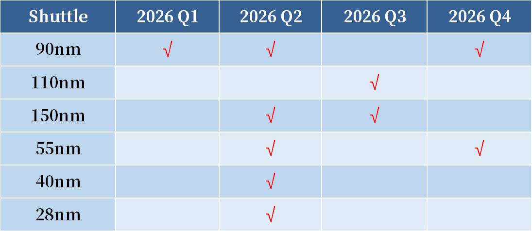
5.MPW
Nexchip provides MPW(shuttle) service for customer to penetrate market rapidly. Customers can verify the prototype design by silicon as soon as possible, and strive for leading market opportunities. Currently, Nexchip shuttle plan is available on the table. If there is a request, please kindly contact sales for details.